
Like other engineering breakthroughs, signal amplifiers originated from an inherent need to solve a problem—extracting accurate data from weak, often noisy signals. Signals from strain gauge load cells, by their nature, are like this. In the millivolts per input volt (mV/V) range, these output signals are highly vulnerable to environmental interference (EMI) and other noise sources. Signal conditioners amplify, filter, and linearize these raw load cell signals, enabling them to drive control systems accurately and present data in human-readable formats.
Before exploring the core methods of signal conditioning, this guide breaks down the foundational analog-to-digital (ADC) and digital-to-analog (DAC) conversions that power these devices. It then concludes with a comparison table and buying guide to help you select the perfect amplifier for your application.
Key Takeaways
- Raw load cell signals require critical intervention: Inherent millivolt-per-volt (mV/V) outputs are too weak to drive control systems and are highly vulnerable to electromagnetic interference (EMI).
- Modern processing relies on digital conversion: Analog-to-Digital Converters (ADCs) are foundational to signal conditioning, with sampling rate and bit resolution establishing the digital signal’s accuracy.
- Conditioners perform up to six core functions: Amplification, attenuation, isolation, linearization, bridge completion, and filtering, together transform weak, noisy electrical data into steady, readable formats.
- Proper selection and installation dictate performance: Matching the correct signal conditioner to your specific load cell and environment ensures precise, distortion-free measurements. Our comparison table illustrates the differences in features of the amplifiers in our catalog.
Analog and Digital Signals: What is the Difference?
Until somewhat recently, load cell signal processing had been mostly analog. However, the majority of modern-day, real-time signal processing systems are entirely digital and software-based.
What is the practical tradeoff? Whereas analog processing is instantaneous and cost-effective, digital processing provides higher accuracy, easier tuning, and simplified troubleshooting. The latest digital signal processors also have negligible latency thanks to ever-increasing processor speeds. However, hybrid systems that combine both remain a choice when balancing cost and hardware performance.
How Does Analog-to-Digital Conversion (ADC) Work in Weigh Systems?
Analog-to-Digital Converters (ADCs) transform the continuous voltage output of a load cell into discrete digital data. This conversion is essential for efficiency in modern weigh systems since digital signals are much easier for microcontrollers and software to manipulate, filter, and transmit than raw analog data.
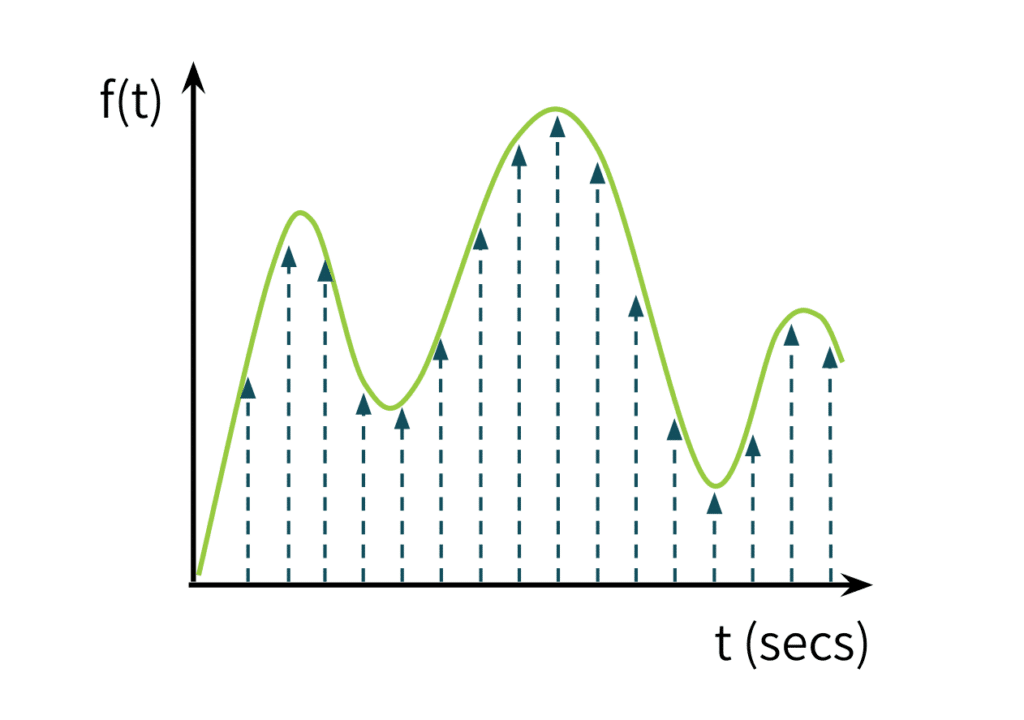
To achieve this, the ADC performs discrete time sampling. As illustrated in Figure 2, the ADC measures the amplitude of the continuous analog signal (the light green curve) at specific, regular intervals in time. This is known as the sample rate. Each sampled data point (represented by the arrows) is then translated into a string of digital bits representing the discrete value of the analog signal’s magnitude at that moment. This string creates a data stream that digitally approximates the weigh system’s output.
It is important to note that the number of bits representing the digital sample (or bit resolution) and the sample rate can vary. The next sections discuss how signal accuracy varies with bit resolution and sample rate.
How Does the Sampling Rate Affect Signal Accuracy?
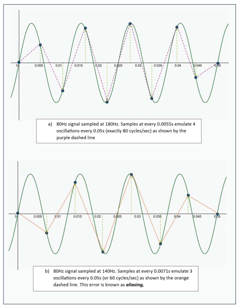
According to the Nyquist-Shannon Theorem, ADC sampling must occur at least twice the frequency of the highest analog signal frequency to avoid distortion. That is,
\(f_{s}\) > \(2 f_{max}\)
Where \(f_{s}\) is the sample frequency and \(f_{max}\) is the highest frequency in the signal. The converse is also true. That is, the factor \(f_{max}\) cannot exceed the ADC’s “Nyquist limit,” or half of its sampling frequency. That is, if an ADC samples at 120 samples per second, the highest input frequency that the ADC output can accurately represent is 60 Hz.
When the highest analog frequency is above the Nyquist limit, the digital signal will present an error known as aliasing. That is, the samples represent random points that mimic a lower frequency signal.
How Does Bit Resolution and Quantization Error Affect Signal Accuracy?
Equally important to the sampling rate, the ADC’s bit resolution establishes the accuracy of the digital amplitude, or signal strength. An ADC typically uses a minimum of eight bits to represent the data, where each additional bit exponentially increases the converter’s resolution:
28 = 256, so the resolution of the 8-bitsample is 1 part of 256
212 = 4096, so the resolution of the 12-bit sample is 1 part of 4096
Higher bit resolution directly increases the system’s dynamic range (the span between the smallest and largest measurable signals). It therefore lowers the quantization error (the mathematical difference between the actual analog input and its digitized approximation). For example, when reading a 100 mV signal, an 8-bit ADC divides the range into 256 discrete, digitally represented steps of roughly 0.39 mV. Because the system rounds to the nearest step, the digitized value will never be more than 0.195 mV (half a step) away from the true analog voltage. Upgrading to a 12-bit ADC shrinks those steps to 0.024 mV, shrinking the maximum quantization error to a far smaller 0.012 mV.
Signal Conditioners: What Are They and What Do They Achieve?
With this understanding of sampling and the mV range of the load cell output, it is easy to see how EMI and other unwanted additive frequencies would create a very low Signal-to-Noise Ratio (SNR) and distort this output’s digital approximation. Signal conditioning “cleans up” the raw measurement signal to give it these three usable qualities:
- It will be large enough to detect (through amplification),
- It will be free of noise/unwanted frequencies (through filtering), and
- It will be in the appropriate signaling format.
This section will explain each of these 6 Core Functions of Load Cell Signal Conditioning in more detail:
- Amplification: Boosts the raw millivolt (mV/V) signal to standard usable ranges, such as 0-10V or 4-20mA, using operational amplifiers (op-amps).
- Attenuation: Decreases signal amplitude when the voltage exceeds the safe input range of the analog-to-digital converter (ADC).
- Isolation: Protects the measurement system from dangerous voltage spikes, breaks ground loops, and blocks electrical surges.
- Linearization: Corrects non-linear sensor outputs into proportional, linear signals for accurate measurement across the entire scale.
- Bridge completion: Provides the necessary high-precision resistors to form a complete four-wire Wheatstone bridge when using quarter or half-bridge strain gauges.
- Signal Filtering: Utilizes high-pass, low-pass, band-pass, or notch filters to strip environmental electrical noise (like power line frequencies) from the raw data.
(1) Amplification: Analog and Digital
How does an instrumentation amplifier change the load cell’s raw signal? It amplifies the load cell output from 0~36 mV to either 0-10V or 4-20mA. Amplifiers typically use DC power (24V) and can drive ~ 300Ω load cells connected directly. Many handle one or two devices alone, but can connect to more load cells at a time via junction boxes. (See Load Cell Summing: Junction Boxes, Signal Trim and Excitation Trim.)
Analog Amplifiers
Typically analog amplification happens through an operational amplifier, also known as an op-amp. Op-amps are electronic devices with two input terminals: the inverting and non-inverting ends. As Figure 4 shows, the raw signal connects to the inverting side with one resistor; the non-inverting side connects to ground. A feedback path connects from the output terminal, with a second resistor, to the inverting terminal.
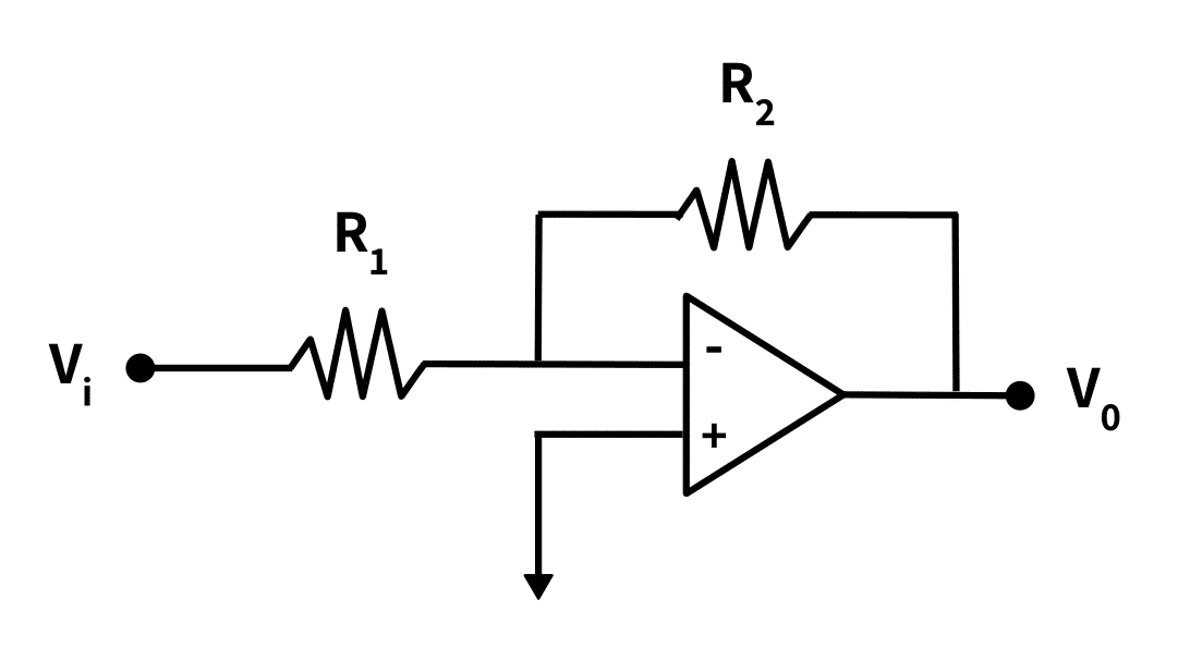
The output signal is related to the input voltage through the equation below. Therefore the amount of amplification is based on the values of R1 and R2.
Operational Amplifier Relational Equation
\(V_{0}= – \frac{R_{2}V_{i}}{R_{1}}\)
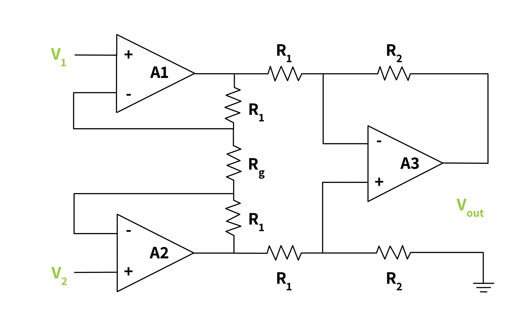
Load cell outputs require instrumentation amplifiers that combine up to three op-amps. This is because load cells do not output a single voltage relative to ground. Instead, they output a differential signal across two distinct wires (a positive signal and a negative signal). A single op-amp struggles to measure the difference between these two wires without adding background noise. The 3-op-amp Instrumentation Amplifier (Figure 5) is specifically designed to measure the difference between those two wires while perfectly canceling out any shared electrical noise (like the EMI we discussed earlier).
Certain applications, like accelerometers, require the amplifier to have a high-frequency response, to prevent distortion.
Digital Amplifiers
Digital amplifiers, as the name implies, increase the magnitude of a digital signal rather than an analog one. When using these, the load cell’s analog output is converted to digital through an ADC before amplifying the signal. The digital amplifier then multiplies the sampled values by a fixed constant to amplify the signal.
(2) Attenuation
Attenuation is the opposite of amplification. Instead of increasing the signal amplitude, attenuation decreases it. This is necessary when a voltage is beyond the range of the device receiving the signal. Like digital amplification, a digital attenuator multiplies the digital signal by a fixed constant, mathematically changing the output’s amplitude.
(3) Isolation
Signals outside of the voltage range of an input device can cause equipment damage and hazards to operators. Isolation is common when there is a need to protect the measurement system from incidental voltage spikes. It also breaks ground loops, blocks surges, and rejects high voltages.
Various methods exist for isolating voltages, including creating physical barriers for signals, and using isolation amplifiers. The specific application, and the driving reasons for the need for isolation determine the method used.
(4) Signal Linearization
Signal linearization converts a transducer’s non-linear output into a linear signal to more accurately represent the measured value. This step is important when the relationship between a sensor’s input and output isn’t perfectly proportional. Devices that measure temperature, such as thermocouples, often need linearization to produce accurate readings across their full range.
Linearization can be done using analog signal conditioning, such as operational amplifiers, or through digital processing in software or microcontrollers.
(5) Bridge Completion
Bridge completion forms a four-resistor Wheatstone bridge when using a quarter or half-bridge sensor. The Tacuna Systems precision strain gauge amplifier/ conditioner provides this function with high-precision resistors. This device detects small voltage changes across the active sensors connected to it.
(6) Signal Filtering
Signal filtering removes unwanted frequencies from a raw signal. An example of these unwanted frequencies is the 60 Hz electromagnetic noise generated by nearby power lines. Because a load cell is typically measuring a static or slow-changing physical weight (a low-frequency signal), a weigh system designer will use a low-pass filter. This filter allows the low-frequency weight data to pass through to the controller, while blocking out the higher-frequency electrical noise.
Signal filtering is possible both digitally and through analog circuits. The most common filters are high-pass, low-pass, band-pass, and notch filters. As their names suggest, these filters allow high, low, mid, or only high/low-frequency signals from the raw source signal to pass, while denying the rest. The range of permitted frequencies is called the passband, while the denied frequency range is called the stopband.
A passive filter uses only passive elements such as resistors, capacitors, inductors, and transformers. Therefore, it does not require an external power source. It has the added advantage of having a more stable output than an active filter.
An active filter, on the other hand, includes active components such as amplifiers and therefore requires a power source. Active filters can provide signal gain and better control over filtering characteristics, making them useful in many precision measurement systems.
How to Choose and Connect a Load Cell Amplifier or Conditioner
While choosing the appropriate load cell model for an application is important, selecting a signal conditioner is equally critical. The wrong amplifier or conditioner can distort the load cell measurements. Likewise, using the load cell amplifier properly is essential for high-quality, accurate readings.
For best results in using signal conditioners, follow these three guidelines.
- Always follow the manufacturer’s operation manual,
- Ensure that operators receive proper training prior to installation,
- Contact your vendor should questions or concerns arise while operating products.
Tacuna Systems is readily available to answer any design or implementation questions regarding our amplifier and conditioner products. See our “Featured Customer Projects” section to see the scope of projects we’ve assisted with.
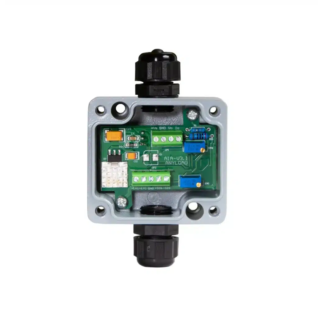
Connecting and Installing a Load Cell Amplifier
The following is an example of connecting an ANYLOAD load cell amplifier:
- The input voltage should connect to 24V DC power and the ground terminal to the ground.
- The load cell connects to the amplifier through the positive(+) and negative(–) excitation terminals, and to the positive(+) and negative(–) output mV signal terminals.
- The output from the amplifier connects to either the current output for a signal of 4~20mA or a voltage output signal of 0~10V.
- To calibrate the Zero (or tare) of the conditioner, remove any load and adjust the “zero” variable resistor to an output of 0V or 4mA. To calibrate the full Span, place the entire load on the transducer and adjust the span variable resistor to an output of 10V or 20mA.
The load measurement system will be fully functional and ready to operate. Re-calibrate the device frequently and whenever the output readings change, or the signal is abnormal. Most load cell signal conditioners should operate from 10°C – 40°C, or 15 – 100°F, and below 90% relative humidity. However, always review the product specs before operating in high and low-temperature environments.
Lastly, contact the supplier for setup assistance, calibration assistance, and troubleshooting.
Tacuna Systems Load Cell Amplifiers: Comparison and Buying Guide
This section provides a comparison table with each amplifier and signal conditioner product Tacuna Systems carries.
| Device | Tacuna Systems EMBSGB200-C | Tacuna Systems EMBSGB200-X | ANYLOAD A1A-22B | ANYLOAD A1A-D25 | ANYLOAD A1A-D25C | ANYLOAD A2A-D2 | ANYLOAD A2P/A2P-D2 | DGB–A | DGB-D |
|---|---|---|---|---|---|---|---|---|---|
| Input Signal | 100mV DC | 100mV DC | 0mV-30mV | 0.8~3.9 mV/V | 0.8~3.9 mV/V | 0±36mV | 0±36mV | 0.2–10.0 mV/V | 0.8 – 3.9 mV/V |
| Excitation voltage to LC | 5V | 5V | 12V | 5V | 5V | 5V or 12V (settable) | 5V or 12V (settable) | 5V | 5V |
| Output Signal | 0-5V analog, 4-20mA | 0-5V analog or 12 bit digitized with ADC | 0-10V, 4-20mA | Digital RS-232 or RS-485 | Digital RS-232, RS-485, or CAN Bus | 0±10V, 4-20mA | 0±10V, 4-20mA | 0-20 mA, 4-20 mA (for the DGB-AI2508B) or 0-5V, 0-10V, ±5V (for the DGB-AV2508B) | Digital RS-232, RS-485, or CAN Bus |
| Capacity | With junction box up to: 16 x 700Ω 8 x 350Ω | With junction box up to: 16 x 700Ω 8 x 350Ω | Single 350Ω or With junction box up to: 8 x 700Ω 4 x 350Ω | Single 350Ω or With junction box up to 4 x 350Ω or greater | Single 350 Ω or With junction box up to 4 x 350 Ω or greater | 1 or 2 directly-connected 350Ω or With junction box up to: 8 x 700Ω 8 x 350Ω 4 x 350Ω | 1 or 2 directly-connected 350Ω or With junction box up to: 8 x 700Ω 8 x 350Ω 4 x 350Ω | Single 350Ω at 12V DC or 2×350Ω at 24V DC | Single 350 Ω or With junction box up to 4 x 350 Ω or greater |
| Bridge Completion | Yes: 1/4, 1/2, 3/4, and full bridge | Yes: 1/4, 1/2, 3/4, and full bridge | No | No | No | No | No | No | No |
| Power Supply | 8-24 V DC | 8-24 V DC | 24 V DC (±10%) | 6-24 V DC | 9-24 V DC | 24 V DC (± 20%) | 24 V DC | 12 – 24 V DC | 9 – 24 V DC (0.36W consumption @ 12 V) |
| Communica- tion Protocols | NA | RS-232 | Analogue to IO-Link compatible (Balluff’s IO-Link modules) | RS-232 or RS-485 (using MODBUS protocol) | RS232, RS485 (Modbus RTU), or CAN Bus (CANOpen / J1939) | NA | NA | NA | RS232, RS485 (Modbus RTU), or CAN Bus (CANOpen) |
| Noise Elimination Filter | Two low-pass (corner frequency ~70Hz with 350Ω bridge or ~100 Hz with 120Ω bridge) | One low pass antialiasing filter; corner frequency 200Hz | Internal digital filter | Internal digital filter | 2.3Hz | Built-in Anti-EFT (Electrical Fast Transient pulses) and anti-radiation interference | Built-in internal digital filter (with programmable FIR filter levels and stabilization bands) | ||
| Operating Temperature | -14°F to 104°F / -10°C to +40°C | -22°F to +176°F / -30°C to +80°C | -22°F to 122°F / -30°C to +50°C | 14°F to 122°F / -10°C to +50°C | 14°F to 122°F / -10°C to +50°C | -22°F to 122°F / -30°C to +50°C | -22°F to 122°F / -30°C to +50°C | ||
| Accuracy | 0.1% Max Gain Error (0.03% Typical) | 0.1% Max Gain Error (0.03% Typical) | ≤ 0.02% Non-Linearity | ≤ 0.01% Non-Linearity | ≤ 0.01% Non-Linearity | ≤ 0.02% Non-Linearity | ≤ 0.02% Non-Linearity | ≤ 0.02% Non-Linearity | ≤ 0.01% Non-Linearity |
| Gain Setting | Discrete preset values selectable with DIP switch | Programmable via RS232 | SPAN Potentiometer | Digital; Programmable via RS232 | Digital; Programmable | SPAN Potentiometer and combination of DIP switch and excitation voltage settings | SPAN Potentiometer and combination of DIP switch and excitation voltage settings | Software Programmable via USB | Digital programmable (Supports up to 9-point linear calibration written via software/Modbus registers) |
| Offset Adjustment | Potentiometer | Programmable via RS232 | ZERO Potentiometer | Programmable via RS232 | Digital | Zero Potentiometer (Plus IN1 and IN2 Pots when 2 LCs are directly connected) | Zero Potentiometer (Plus IN1 and IN2 Pots when 2 LCs are directly connected) | Software Programmable via USB | Digital programmable (Zero tracking and tare values written via software/Modbus registers) |
| Field Calibration Required? | No | No | Yes | Yes (9pt multi-section, non-linear calibration) | Yes via Modbus RTU Protocol (9pt linear calibration) | Yes | Yes | Yes via DGB-WIRE-25A USB tool | Yes (Requires sending digital commands from a PLC or PC software while applying known weights) |
| Overall Dimensions | 1in x 3in x 0.5in | 1in x 3in x 0.5in | 3.7in x 2.5in x 1.4in | 3.7in x 2.5in x 1.4in | 3.7in x 2.5in x 1.4in | 4.02in x 5.0in x 1.14in | 3.9in x 2.8in x 2.6in | 2.52in x 1.21in x 0.61in | 2.52in x 1.21in x 0.61in |
| Enclosure Material | ABS (optional) or directly embedded | ABS (optional) or directly embedded | Aluminum Casting | Aluminum Casting | Aluminum Casting | Aluminum Casting with a preinstalled GORE protective vent | PVC | Optional or directly embedded | Optional or directly embedded |
| Enclosure Ingress Protection | IP40 | IP40 | IP66 | IP66 | IP66 | IP66 | IP40 | IP40 | IP40 |
| Enclosure Installation | None – Tabletop or double-sided tape | None – Tabletop or double-sided tape | 2 Screw mounting holes within enclosure | 2 Screw mounting holes within enclosure | 2 Screw mounting holes within enclosure | 4 Screw mounting holes within enclosure | DIN rail mounting | 24.6mm diameter center chip can be embedded within load cells or 2 through-holes on PCB base | 24.6mm diameter center chip can be embedded within load cells or 2 through-holes on PCB base |
Summary
The weak load cell output signal is easily distorted by environmental noise and too small to drive a readout or control system. Therefore, accurate weigh systems incorporate signal conditioning, including amplification, filtering, and linearization. These improve signal quality to ensure precise, consistent measurements.
A properly conditioned output should be:
- Strong and stable enough for accurate processing by displays, controllers, or data systems
- In the correct format (analog or digital)
- Filtered to remove unwanted frequencies (noise-free)
To see an interesting example of our Tacuna Systems EMBSGB200 Amplifier at work, see Next-Gen Transmissions for High-Performance Hybrid Cars in our “Featured Customer Projects” section of this Knowledge Base. Also, see Measuring Contact Forces on Soft Materials for Medical Robotics and Other Applications, and How the EMBSGB200 Amplifier is Shaping Innovations in Technology and Industry, for other examples of how our customers have used this versatile device.
References
- Measurement and Instrumentation Principles, 3rd Edition, Alan S. Morris
- The Engineer’s Guide to Signal Conditioning, National Instruments
- Product Manuals for all products mentioned