
Have you ever wondered how the appliances and gadgets you use at home, workplace, or industry operate? To a large extent, they employ the piezoelectric effect in materials. This article explains this effect in detail, including common piezoelectric materials and their fabrication process. It also describes uses for the piezoelectric effect in piezoelectric nanomaterials (PN), energy harvesting devices, piezoelectric sensors, and actuators.
Key Takeaways
- The piezoelectric effect generates electric charges through mechanical stress on specific materials.
- Common piezoelectric materials include naturally occurring crystals like quartz and man-made materials like lead zirconate titanate (PZT).
- This effect finds applications in areas such as energy harvesting, sensors, and actuators.
- Piezoelectric nanomaterials enable advancements in nanoelectronics and smart devices, enhancing their efficiency.
- The article covers fabrication processes and various applications, highlighting the practical implications of piezoelectric effects.
The Piezoelectric Effect – What Is It?
The term “piezoelectric” is a compound word that is derived from the Greek words: “piezein,” meaning “to press or squeeze;” and “elektron,” meaning “amber” and referring to an alloy of gold and silver used in ancient times, from which all electrical conductors are named. Therefore, it follows that the piezoelectric effect describes the production of electric charges when a piezoelectric material experiences elastically deformational stress.
The Piezoelectric Effect – How It Works
The piezoelectric effect occurs in a crystalline structured material when it experiences a mechanical strain. Piezoelectric materials have polarity in steady state; this means finely aligned electric dipoles exist inside the material. A strain causes a misalignment of the dipoles, or depolarization of the material.
The initial polarization causes a stable electric field, while the change in polarization results in a change in the dielectric field. The piezoelectric effect is an AC phenomenon.
The equations below describe this effect mathematically. The simultaneous equation uses tensor parameters to describe mechanical behaviors and the electric field.
\(\vec{S}=\)
\(s^{E}\vec{T}+d_{2}\vec{E}\)
\(\vec{D}=\)
\(d_{1}\vec{T}+\epsilon ^{T}\vec{E}\)
\(\vec{D}:\)
\(dielectric\: displacement\)
\(d_{1},d_{2}:\)
\(piezoelectric\: charge\: coefficients\)
\(\vec{T}:\)
\(mechanical\: stress\)
\(\epsilon ^{T}:\)
\(permittivity\: at\: constant\: stress\)
\(\vec{E}:\)
\(electric\: field\)
\(\vec{S}:\)
\(mechanical\: strain\)
\(S^{E}:\)
\(mechanical\: compliance\)
The first equation depicts the transformation of an electric field into mechanical strain. Therefore, in the absence of an electric field, it becomes a function of mechanical stress only. This shows the relationship between the distortion and the applied stress for an elastic material, or Hooke’s law.
The second equation describes the change in electric field due to mechanical strain. Therefore, in the absence of mechanical stress, it is a function of the electric field only. For a dielectric substance, this depicts the relationship between the electric displacement and the electric field strength.
Now, the charge coefficient for the direct piezoelectric effect and that of the reverse piezoelectric effect are nearly equal for the same material. Consequently, they are both approximately equal to d. With this in mind, manipulating both equations gives:
\(\vec{S}=\)
\(s^{E}(1-k^{2})\vec{T}+\frac{d}{\epsilon ^{T}}\vec{D}\)
\(k^{2}=\)
\(\frac{d^{2}}{s^{E}\epsilon ^{T}}\)
…where \(k\) is called the electromechanical coupling coefficient. It shows the efficiency of the material in converting electric energy into mechanical energy and vice-versa. That is the materials efficiency for a piezoelectric effect and for a reverse piezoelectric effect.
Piezoelectric Material Categories
Piezoelectric materials can be classified into two categories:
- Naturally occurring crystals such as Quartz, Topaz, Tourmaline, Rochelle salt, and cane sugar.
- Man-made materials such as lithium sulfate, polarized ferroelectric ceramics such as the lead zirconate titanate (PZT), polyvinylidene fluoride (PVDF).
Man-made Piezoelectric Material Fabrication Process
The synthetically made piezoelectric materials are generally fabricated through the process called poling [4]. The steps are as follows, at a high level:
- Fine powders of different metal oxides are mixed in specific proportions and then heated. This forms a piezoelectric powder that is then mixed with an organic binder and formed into structural elements of a desired shape – discs, rods, plates, etc.
- The element is then heated to a temperature above the Curie point, where the ferromagnetic properties of the crystal break down.
- The heated material is then allowed to cool under a strong DC electric field. This ensures the alignment of all the dipoles in the material. The direction of alignment is determined by the direction of the applied electric field and the field strength.
Applications of the Piezoelectric Effect
Applications of the piezoelectric effect cover a wide range. Some of these are include development of piezoelectric nanomaterials, design of energy harvesters, piezoelectric sensors, and actuators. This section explains each.
Piezoelectric Nanomaterials
Research involving the application of the piezoelectric effect at nanoscale is broad. This has created what is called the piezoelectric nanomaterial (PN) [5].
PNs are a class of nanomaterials and are the basis for the design of smart nanodevices and nanoelectronics. According to [6], PNs are potential elements in making smart nanopiezoelectronics such as nanoresonators, nanosensors, nanoactuators, and nanogenerators.
The research in this area of material science necessitates the development of new fabrication techniques. It also has derived new theories other than those applicable to normal piezoelectric effects. The characteristics of the piezoelectric effect at the macroscale are different at the nanoscale; these new better describe and interpret the behavior of PN at the nanoscale.
The types of PNs, their applications, and methods of fabrication are as follows [5]:
Three-Dimensional PNs
These materials are available at both the macroscale and the nanoscale. They include:
- Perovskite: PNs with Perovskite crystal structures are commonly fabricated with piezoelectric ceramics such as PZT. They appear in applications such as electromechanical sensors, actuators, and energy generators. There are also Perovskite Nanostructures that exhibit both piezoelectricity and ferroelectricity. This lends them to phased-array radar and ferroelectric memory applications. Fabrication methods for these materials include the Sol-gel template method, electrospinning, and sheet casting.
- The Wurtzite Structure: These PNs are made from materials such as ZnO, GaN, Indium Nitride, Zinc Sulfide. They exhibit less piezoelectric effects than the Perovskite types. However, they possess a synergy of piezoelectric and semiconducting properties called the nanopiezotronic effect. This makes them useful for piezoelectric nanogenerators, nanotransistors , and nanodiodes. The fabrication technique applied in their design is the hydrothermal method.
Two-Dimensional PNs
These materials are available only at the nanoscale and are classified into three groups.
- The single-atom layer of boron nitride nanotubes that can be used in developing smart nanomaterials. Its fabrication method includes arc discharge and laser-ablation.
- The family of trigonal-prismatically coordinated transition metal dichalcogenide crystals. They possess stronger piezoelectric effects than Wurtzite materials. Their fabrication techniques include mechanical exfoliation and chemical vapor deposition.
- Chemically modified graphene (carbon nanosheets). They have a zero band gap semi-metallic behavior and excellent mechanical responses, but they are intrinsically non-piezoelectric. To induce piezoelectricity in these materials, the fabrication causes the graphene sheets to adsorb atoms on one of its sides.
Energy Harvesting Applications
Research is ongoing and prototypes exist for the extraction of waste energy from the environment using the principles of the piezoelectric effect. Actually, they employ the reverse piezoelectric effect. Some of these endeavors involve the collection of vibration energy produced by the movement of vehicles on the road or fixed mechanical equipment. Others aim to collect energy from waste heat sources such as electronic chips.
Most piezoelectric energy harvesting devices chiefly operate in two modes [7].
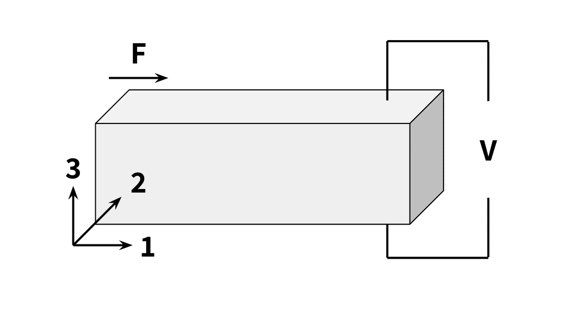
- The 33-mode, shown in Figure 1a below, is where the applied stress’ direction aligns with that of the generated voltage.
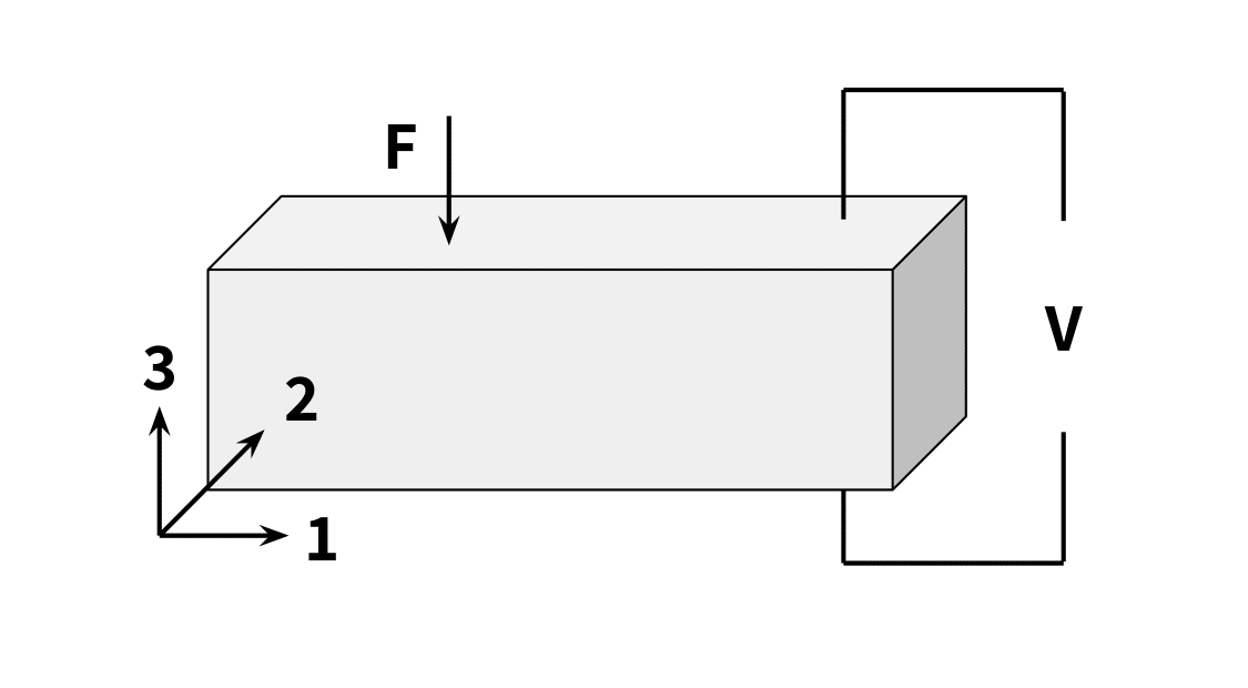
- The 31-mode, shown in Figure 1b, is where the direction of the applied axial stress is orthogonal to that of the generated voltage.
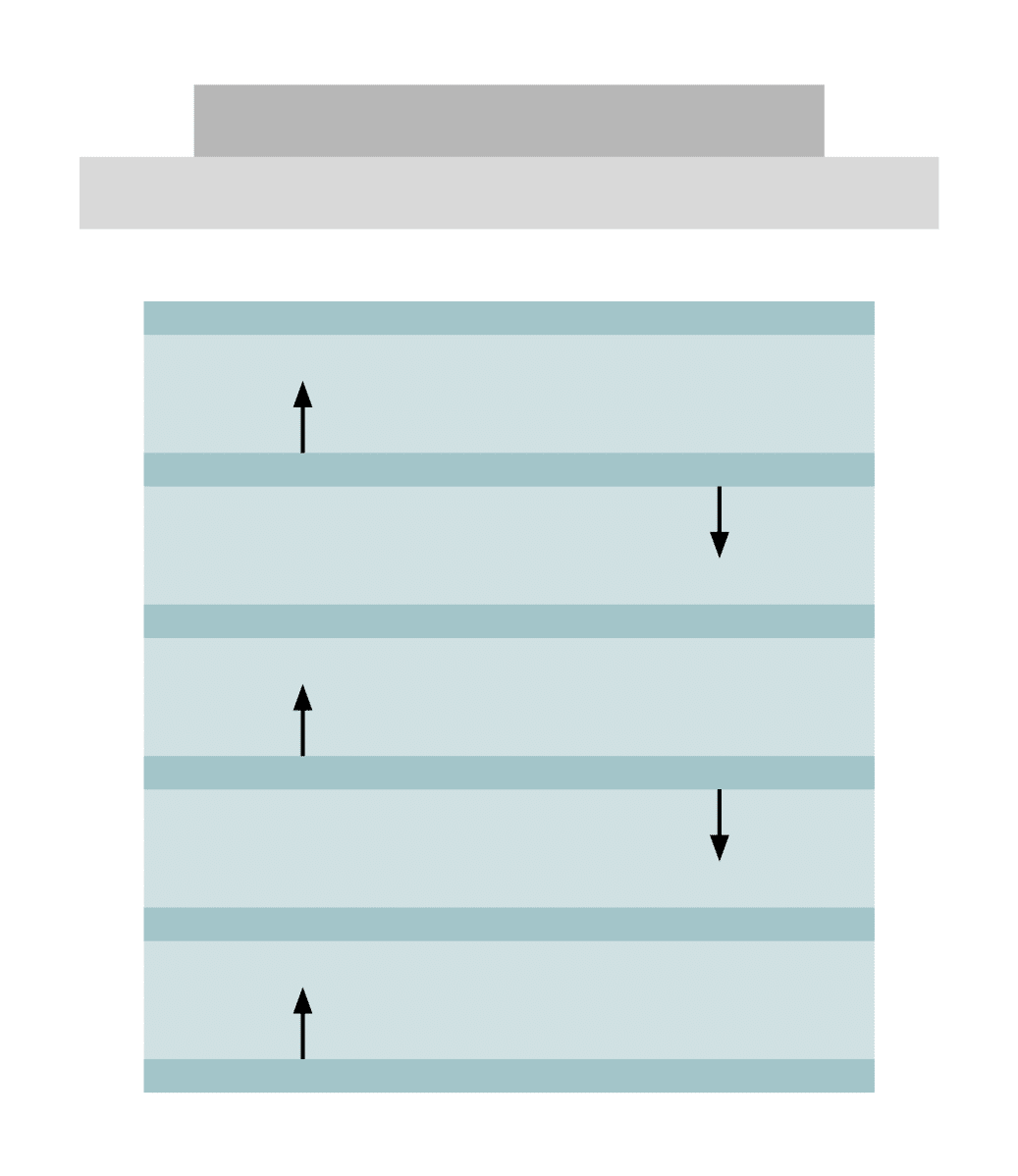
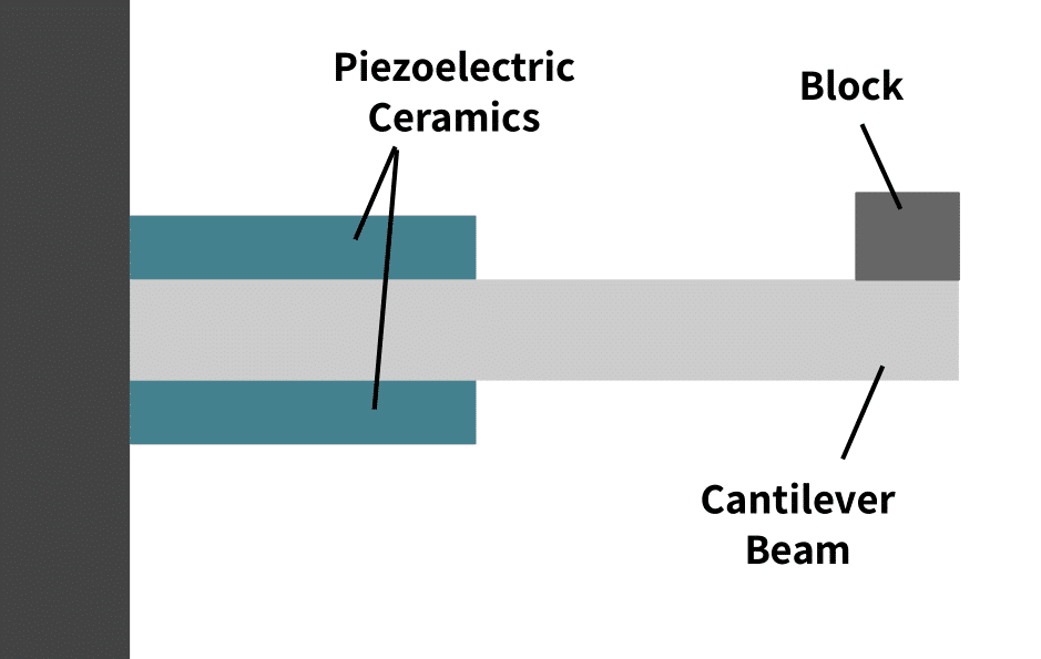
Furthermore, the common structural design of these devices falls into three categories. These are: stacked, cantilever beam, and cymbals, per Figures 2-4 respectively [7].
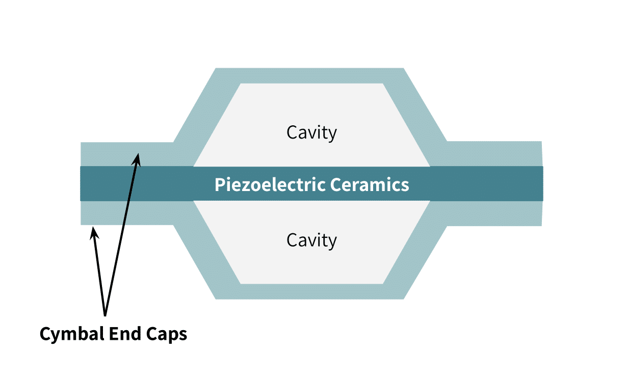
This research has produced some interesting results: A piezoelectric transducer box embedded experimentally in roads, and a road energy harvesting system that produces 250kW of electric power (Israel) [7], a piezoelectric floor that lights up office LEDs (Japan), and finally a thermal energy harvester that combines the piezoelectric effect and pyroelectric effect [8].
Piezoelectric Sensors
These are macro scale level devices that employ the piezoelectric effect to provide solutions to industrial practical problems. It should be noted that these devices are passive – they are powered only through the applied input stimulus. This section introduces some of these sensors, their principle of operation, structural design, and applications.
Piezoelectric Tactile Sensors:
Tactile sensors are generally fabricated from PVDF and can operate in either passive or active modes depending on the application.
Figure 5 below shows the design of an active piezoelectric tactile sensor. The structural design places the PVDF film between a central compression film made of silicon rubber. The figure below shows their amplifier and demodulator setup.
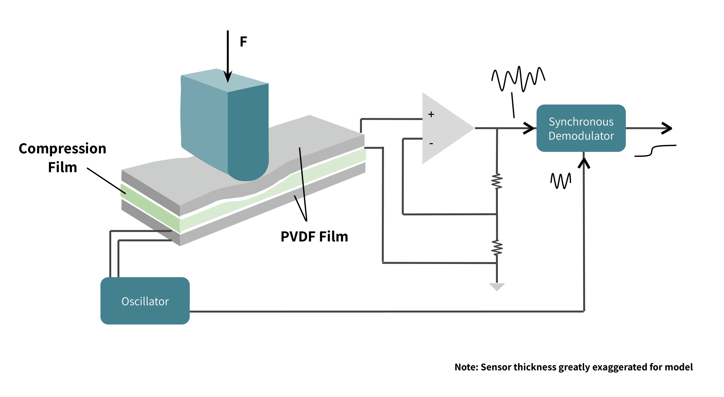
These operate on the principle that if the upper film experiences a mechanical compressive force, the device generates a voltage. This signal then becomes the amplifier input. Simultaneously, the compression force transmits through the silicone rubber to the bottom film; this film also generates a voltage signal to the demodulator. The combined signaling produces the appropriate output AC voltage.
These devices appear in electronic musical instruments such as electronic pianos. They are also applicable in robotics for detecting colliding motions or sensing grip pressure.
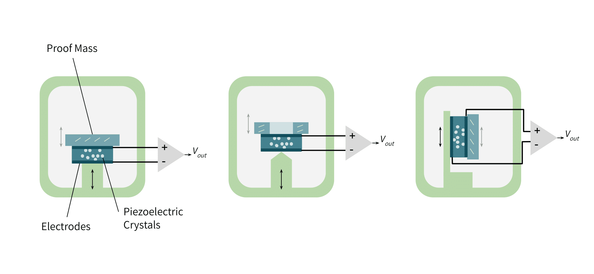
Piezoelectric Accelerometers:
This is a type of linear accelerometer that works by attaching to a moving platform; it does not require a stationary coordinate system. This device employs Newton’s second law of motion. Its structure contains a piezoelectric material sandwiched between a supporting structure and a proof mass; the proof mass couples directly to the piezoelectric material and exerts a force proportional to the acceleration.
There are various configurations for mounting the piezoelectric material and the proof mass on the accelerometer housing. These configurations are the compression coupling (a), the flexural coupling (b), and the shear coupling (c). See Figure 6 below.
Piezoelectric Force Sensors:
These are also called piezoelectric force transducers. They transform an applied force into a varying electrical charge output. There are quite a few ways through which the output can be detected and measured.
- The output can be amplified using a charge amplifier.
- The output can integrate as a resonator in an electronic oscillator.
There is more information about the design, fabrication, and principle of operation of these devices in [9]. They exist in pinball machines as a roll-over type switch, in natural gas meters as shaft rotation counters, in electric utility metering as gear tooth counters, and in textile manufacturing to monitor thread breakage.
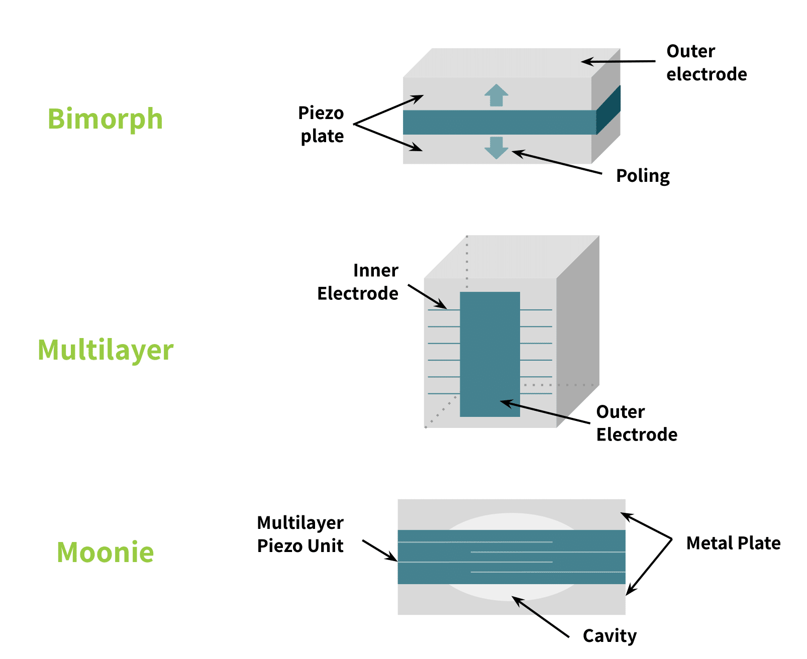
Piezoelectric Actuators
These devices use the principle of the reverse piezoelectric effect. Their applications fall into three classes of smart actuators systems [10]:
- Positioners
- Motors
- Vibration Suppressors
Some of the most common designs for these devices are the multilayer, bimorph, and moonie structures. These designs appear in Figure 7 below.
Conclusion
This article discussed the piezoelectric effect and its various applications cutting across nanoscience, energy harvesting, force sensing, and actuator systems.
There are many addition applications of the piezoelectric effect, including piezoelectric cables, ultrasonic sensors, airbag sensors, ceramic filters and resonators, piezoelectric buzzers, and piezoelectric transformers. These were not specifically described since they all follow the same working principles as most of the devices listed in this article. Only their structural design varies. We recommend the references below or further browser searches to explore these other applications.
References
[1]
A. Ledoux, “Theory of Piezoelectric Materials and Their Applications in Civil Engineering,” Massachusetts Institute of Technology, 2011.
[2]
Jacob Fraden, Handbook of Modern Sensors, Springer, 2015.
[3]
Comparing strain gauges to piezoelectric sensors, Tacuna Systems, 2019. [Online].
[4]
Chapman and Hall, Electroceramics: Materials, Properties, and Applications, New York, 1990.
[5]
Jin Zhang, Chengyuan Wang, and Chris Bowen, “Piezoelectric Effects and Electromechanical Theories at The Nanoscale,” Nanoscale, vol. 6, no. 22, pp. 13314 – 13327, 2014.
[6]
Wang ZL, Song J., “Piezoelectric nanogenerators based on zinc oxide nanowire arrays,” Science, vol. 312, no. 5771, pp. 242-246, 2006.
[7]
Xiaochen Xu, Dongwei Cao, Hailu Yang, Ming He, “Application of Piezoelectric Transducer in Energy Harvesting in Pavement,” International Journal of Pavement Research and Technology, vol. 11, pp. 388-395, 2018.
[8]
Miwon Kang and Eric M. Yeatman, “Thermal Energy Harvesting Using Pyroelectric and Piezoelectric Effect,” Journal of Physics: Conference Series, vol. 773, no. 012073, 2016.
[9]
Installing and Mounting Piezoelectric Force Transducers, Tacuna Systems, 2019. [Online].
[10]
Kenji Uchino, “Introduction to Piezoelectric Actuators and Transducers,” International Center for Actuators and Transducers, Penn State University, 2003.